Precise p-type and n-type doping of two-dimensional
- Classification:Chemical Auxiliary Agent
- CAS No.:117-84-0
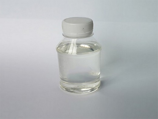
- Other Names:Liquid DOP, DOP oil
- MF:C24H38O4, C24H38O4
- EINECS No.:201-557-4
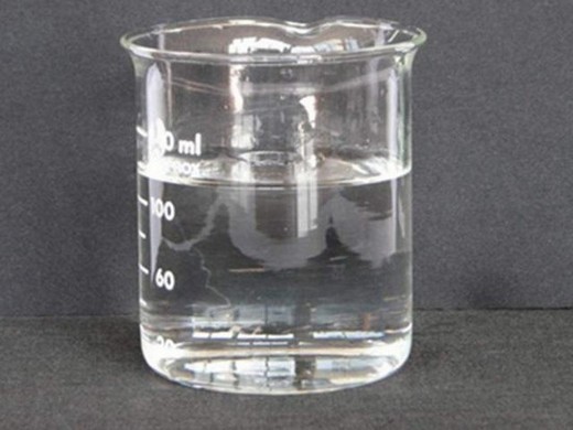
- Purity:99.5%min, 99.5%min
- Type:Adsorbent, Carbon Black
- Usage:Plasticizer
- MOQ:200kgs
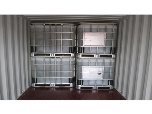
- Package:200kgs/battle
- Place of Origin::China
- Advantage:Stable
In contrast, for 2H-MoTe 2 doped with Re, at low doping levels of 0.06% Re, the channel displayed ambipolar transport behavior, and with increasing doping concentration, the channel exhibited n
There are two main types of semiconductor doping: P-type and N-type. Together, they give rise to an extrinsic semiconductor. 1. P-type. In P-type doping, impurities create an excess of positively charged holes in the crystal
Highly efficient modulation doping: A path toward
- Classification:Chemical Auxiliary Agent
- CAS No.:117-84-0
- Other Names:Chemical Auxiliary Agent
- MF:C24H38O4, C24H38O4
- EINECS No.:201-557-4
- Purity:99.5% Min
- Type:Adsorbent, Carbon Black
- Usage:Leather Auxiliary Agents, Paper Chemicals, Plastic Auxiliary Agents, Rubber Auxiliary Agents, Textile Auxiliary Agents
- MOQ:200kgs
- Package:200kgs/battle
- Place of Origin::China
- Advantage:Stable
Efficient doping for charge-carrier creation is key in semiconductor technology. For silicon, efficient doping by shallow impurities was already demonstrated in 1949 ().In the development of further semiconductor
Conventional semiconductors usually have low to intermediate doping concentrations and small dielectric constant, which together indicate the dominance of the
Why and How Do We Dope Semiconductors?
- Classification:Chemical Auxiliary Agent, Chemical Auxiliary Agent
- cas no 117-84-0
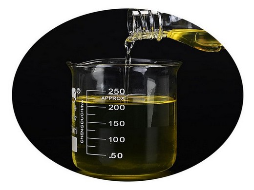
- Other Names:DOP/Dioctyl Phthalate
- MF:C24H38O4
- EINECS No.:201-557-4
- Purity:99.5
- Type:Plasticizer
- Usage:Rubber Auxiliary Agents
- MOQ:200kgs
- Package:200kgs/battle
- Shape:Powder
- Shape:Powder
- Model:Dop Oil For Pvc
The movement or travel of the impurity atoms from a high concentration area to a low concentration area is referred to as diffusion. Pre-deposition and drive-in are the two stages through which the process takes
The essence of an electronic doping effect is a shift of the Fermi level E F toward the highest occupied (p-doping) or lowest unoccupied (n-doping) states 27,28, with the
Heavily Doped Semiconductor Nanocrystal
- Classification:Chemical Auxiliary Agent, Chemical Auxiliary Agent
- cas no 117-84-0
- Other Names:Chemical Auxiliary Agent
- MF:C24H38O4, C24H38O4
- EINECS No.:201-557-4
- Purity:99.5%min, 99.5%min
- Type:Plastic Auxiliary Agents
- Usage:Coating Auxiliary Agents, Plastic Auxiliary Agents, Rubber Auxiliary Agents
- MOQ::10 Tons
- Package:25kg/drum
- Shape:Powder
- Advantage:Stable
- Keywords:Plasticizer Dop
Adding even a single impurity atom to a semiconductor NC with a diameter of 4 nm, which contains about 1000 atoms, leads to a nominal doping level of 7 × 10 19 cm –3.In a bulk semiconductor this is already well within the
Doping, as a primary technique to modify semiconductor transport, has achieved tremendous success in the past decades. For example, boron and phosphorus doping of Si modulates the dominant carrier type
Surface Transfer Doping of Semiconductors
- Classification:Chemical Auxiliary Agent, Chemical Auxiliary Agent
- cas no 117-84-0
- Other Names:DOP, Dioctyl phthalate
- MF:C24H38O4
- EINECS No.:201-557-4
- Purity:99.5, ≥99.5
- Type:Chemical additives, Chemical dop plasticizer 99%
- Usage:Leather Auxiliary Agents, Plastic Auxiliary Agents, Plasticizer
- MOQ:200kgs
- Package:200kgs/battle
- Storage:Dry Place
“Doping” of semiconductors—that is, the local manipulation of their conductivity—is a key technology for electronic devices. Without doping, for example, a gallium nitride sample larger than the White House would be
Increasing the free-carrier concentration in silicon is a pressing issue in modern electronics. The common shallow-level donors like P and As only permit electrically active doping up to
- Does heavy doping affect a bulk semiconductor?
- In a bulk semiconductor this is already well within the heavily doped limit, where metallic (“degenerate”) behavior is expected (20). Heavy doping in bulk semiconductors leads to several effects summarized in Fig. 1A.
- Why do semiconductors have low doping concentrations?
- Conventional semiconductors usually have low to intermediate doping concentrations and small dielectric constant, which together indicate the dominance of the Coulomb potential in governing their electron scatterings and the relative unimportance of the dopant selection (Fig. 2a).
- What is doping in semiconductors?
- The merging of impure particles in a pristine semiconducting material is known as doping. The impure atoms here allude to those that vary from the pure semiconductor. Doping allows researchers to manipulate the conductance of a semiconductor by utilizing the characteristics of a group of elements known as dopants.
- Can two-dimensional semiconductor substitutional doping be used for thin films?
- In this study, we devise a precise method for two-dimensional (2D) semiconductor substitutional doping, which allows for the production of wafer-scale 2H-MoTe 2 thin films with specific p -type or n -type doping.
- What is modulation doping?
- Modulation doping is a widely used doping method in inorganic semiconductors where a heavily doped wide bandgap semiconductor is brought in contact with a narrow bandgap semiconductor. Efficient doping at the heterostructure interface is achieved by charge transfer from the wide bandgap semiconductor to the narrow bandgap semiconductor.
- What are the most successful products based on doping?
- The most successful product so far is the organic light-emitting diode display with a multibillion U.S. dollar market, which are using doping by controlled coevaporation of small-molecule semiconductors and dopant molecules ( 5 ). The microscopy nature of doping in organic semiconductors is strongly different from inorganic semiconductors ( 6 ).